

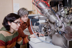
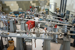
The GCM has numerous devices to characterize the different materials properties. In general, it’s possible to classify these techniques in four large categories:
- Chemical analysis
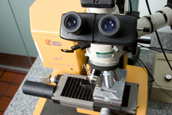
- Microscopy
- Mechanical properties
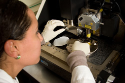
A chemical analysis aim to obtain the sample’s elementary or molecular composition. Different techniques allow to obtain qualitative, semi-quantitative or quantitative results and to analyze liquids, solids and/or gaz. More information is available on the Chemical Analysis page as well as on each different technique’s page.
GCM Lab offers numerous chemical analysis techniques that each have its benefits and limitations. In order to make a choice, one should consider those four fundamental factors: the type of materials that can be analyzed (organic and/or inorganic), the type of information that can be obtained (molecular or elementary), the precision (quantitative or qualitative), the detection limit (%, ppm or ppb) and the depth of analysis (mm, microns or nanometers).
Materials
Some techniques are limited to the analysis of solids or liquids. For example, techniques performed under vacuum are not suitable for the study of liquids.
In addition, most techniques can be used to study either organic OR inorganic materials. In that organics are limited to carbon compounds and a few other elements while inorganics include the other ones, the requirements for a good identification can be very different. For instance, a FTIR spectrometer identifies the chemical groups present in organic materials but is almost ineffective for other materials. On the contrary, EDX analysis only gives elemental information (carbon, oxygen, copper) and thus offers limited assets for the analysis of organics.
information type
A chemical analysis aims to obtain the sample’s elementary or molecular composition. For example, a 100g pyrite analysis will reveal approximately 46.5g of sulfur and 53.4g of steel or 100g of the molecule itself (FeS2).
For a simple inorganic sample, an elementary analysis can sometimes be all that is necessary. However, very often it is not the case for organic or more complex samples. Indeed, elementary analysis of polyethylene would only reveal the presence of carbon and hydrogen, which is not enough information to identify the chemical compound.
Furthermore, industrial samples often contain more than a dozen elements, making molecular analysis extremely useful. For example, in the case of a metallurgical residu containing lead sulphate (PbSO4), copper oxide (CuO) and copper arsenide (Cu3As), the elemental composition will only give a limited information about the compounds present.
Precision
Obviously, the precision of measurements is often critical. Analytical techniques can be:
- Qualitative: Presence or absence of an element or molecule (no numerical answer)
- Semi-quantitative: Numerical results with a large error (ex: 30% +/- 10%)
- Quantitatives: Numerical results with a small error (ex: 30% +/- 1%)
Obviously, higher precision is always a plus but in practice, qualitative measurements are often sufficient.
Detection limit
The detection limit of an instrument is the lowest amount of a molecule or element that can be detected from a blank signal. This limit varies significantly between samples and instruments. For example, the detection limit is approximately 0.1 atomic % for XPS, above 5% for FTIR and between ppm and ppb for TOF-SIMS.
Depth
The chemical information obtained by an instrument can originate from the first atomic layers (extreme surface), the surface (nanometers) or volume (microns and above). Surface information is extremely specific but also subject to contamination. However, it is well-suited to the characterization of thin films or to the creation of concentration depth profiles. Furthermore, different methods can be used to clean surfaces before analysis or remove contamination during data analysis.
 TOF-SIMS is one of the most powerful techniques to analyse solids since it gives the possibility to: image and chemically analyse samples, detect very small concentrations of molecules and elements (ppb) and sputter through samples to create a concentration depth profile (2D or 3D).
In practice, the sample is bombarded with primary ions (generally bismuth or gallium) and secondary ions ejected from the surface are analysed. The flight time of the ions as they travel through the analyzer serves to determine their mass to charge ratio and identify the ionic species, thereby allowing one to establish the composition of the sample’s surface layers.
PARAMETERS
Type of samples: organic or inorganic solids
Type of information obtained: elemental and molecular
Precision: Semi-quantitative
Detection limit: parts per billion (ppb)
Depth of analysis: first atomic layers with the possibility of creating profiles one to two microns deep
Smallest measurable area: around 1 micron in diameter
EXAMPLES
- Identification of surface contaminants
- Surface mapping
- Depth chemical profiles
Advantages
Elemental and molecular analysis
Surface analysis with the possibility of creating profiles
Chemical imaging and mapping
Disadvantages
Semi-quantitative analysis
Comparatively long and complex analysis
Analysis under vacuum
application examples
- Analysis of contaminants in the electronics industry
- Chemical mapping of alloys and minerals
- Detection and identification of greases of the surface of containers
Technical specifications
Elements detected: Hydrogen – Uranium, all the isotopes
Resolution/sensitivity : 0.0001 amu, 108 – 1011 at/cm2 (ppb)
Depth resolution : 1 – 3 monolayers
Lateral resolution : ≥ 100 nm
Measurement temperature = -196 to +600o C
Manufacturer : IONTOF
Model : TOF-SIMS IV
Modèle : TOF-SIMS IV
The XPS, because of its versatility, is the most commonly used technique inside of the GCM to perform chemical analyses. In practice, this method can be used to quantitatively determine the elemental and molecular composition of samples. For example, it can measure the iron concentration in a sample but also determine the compound present (ex: Fe2O3).
This ultra-high vacuum techniques (UHV) analyses photoelectron emitted by a samples after being irradiated by magnesium or aluminum x-rays, as predicted by Einstein’s photoelectric effect.
PARAMETERS
Type of samples: organic or inorganic solids
Type of information obtained: elemental and molecular
Precision: Quantitative
Detection limit: 0.1 atomic %
Depth of analysis: 10 nanometers
Area measured: 2 mm x 3 mm
EXAMPLES
- Quantitative and non-destructive analysis of organic and inorganic materials.
- Identification of contaminants
- Identification of molecules
Advantages / Inconvenients
Application Examples
Technical specifications
Advantages
Quantitative elemental and molecular analysis
Surface analysis (10 nm)
All types of materials (organic, inorganic)
Inconvenients
No imaging
Analysis in vacuum
Surface sensitive (possible contamination)à
Application Examples
- Chemical composition and identification of minerals, alloys, polymers, industrial residues, etc…
- Failure analysis of paints, glues, construction materials.
- Analysis of corrosion and contamination products
Technical specifications
Elements detected : Lithium – uranium
Resolution/sensitivity: 0.1 – 1 at%
Depth resolution : 1 – 10 nm
Lateral resolution : 2 mm
Other characteristics :
depth profiling
Temperature= -196 – 600o C,
Coating and preparation chamber (sputtering or evaporation)
Manufacturer: VG Scientific
Model : ESCALAB 3 MKII
Manufacturer: Kratos
Model : Axis Ultra
FTIR spectroscopy gives information about chemical bonds and molecular structures. This method is particularly useful to obtain the qualitative or semi-quantitative composition and mapping of organic materials.
During the analysis, the sample is irradiated by infrared light that is absorbed by its molecules at wavelengths varying according to vibrational modes. Because of this, an infrared spectrum can be used to identify the compounds present.
PARAMETERS
 Type of samples: Organic liquids and solids
Type of information: molecular
Precision: Qualitative (usually) in limited cases semi-quantitative
Detection limit: about 5%
Depth of analysis: up to 5 microns
Smallest measurable area: 1 micron
Uses
- Identification of the molecular composition on the surface and in depth
- Failure analysis
- Analysis of thin films, coatings and molecular films
Advantages
- Fast and well-know technique
- Mapping available
- Large databases are available to identify a wide range of compounds
- Ideal to quantitatively compare organic materials
Disadvantages
- Generally only useful for organic materials
- Semi-quantitative analyses can be complex
Technical specifications
Resolution/sensitivity : 0.5 cm-1 , 1 – 5% in weight
Depth resolution : 0.1 – 5 µm
Lateral resolution : Imaging : ~ 5 µm
Infrared microscopy (point by point mapping and infrared imaging), photoacoustic cell, depth analysis, horizontal ATR and micro-ATR, specular reflection, diffuse reflection (DRIFTS), PM-IRRAS and variable angle measurements, IR polarization measurements.
Manufacturer : Digilab
Model : FTS7000
Manufacturer : BioRad
Model : FTS6000, FTS3000
An Auger microscope can image samples at very high resolutions and give the elemental chemical composition (semi-quantitative) of an extremely small surface.
Once inside the Auger microscope, the sample is irradiated by an electron beam which causes the ejection of electrons from core levels of the atoms. After this first electron emission, the excited atom can relax by having an electron from a higher energy level fall into the hole left by the first electron and transferring the excess energy to another electron (the Auger electron) which will be emitted from the atom. The kinetic energy of the emitted Auger electrons is a signature of the elements from which they originate. Auger electron spectroscopy has multiple applications like the analysis of particles or defects in various industries such as microelectronics, biomedical and pharmaceuticals.
This microscope is also equipped with an electron backscatter diffraction (EBSD) detector which can be used to determine the crystal orientation at the surface of a sample. It can also be used to map a surface to obtain information about the crystalographic texture, pole figures, grain size. Moreover, because this system is in a ultra high vacuum chamber, it is perfectly suited for the analysis of materials composed of very small grains which often require longer analysis times.
ANALYSIS PARAMETERS
 Materials: Inorganic solids
Type of information: Elementary, limited possibilities for chemical state
Precision: Semi-quantitative
Detection limit: 0.1% to 1 % atomic
Analysed depth: 5 nm, with possibility of depth profiling over one micron
Lateral resolution: around 10 nm
Use
- Analysis of thin film composition
- Analysis of defects
- Surface analysis
- Composition depth profile
- Crystallographic analyses
Advantages
- Analysis of very small regions (10 nm to microns)
- Semi-quantitative analysis
- High resolution imaging
- Determination of the oxidation state possible for some elements
Disavantages
- Elemental composition only (limited information for organic compounds)
- Analysis performed under ultra high vacuum
Application examples
Example 1
Auger electron spectroscopy can be used to distinguish elementary silicon (Si) and oxidized silicon (SiO2). Therefore, by Auger microscopy, it is possible to image the surface of an electronics chip and detect the distribution of Si and SiO2.
Example 2
Auger electron spectroscopy (AES) is a technique which is complementary to energy dispersive X-ray spectroscopy (EDX) often used in combination with scanning electron microscopy (SEM) for element identification. For instance, while EDX is not very sensitive to light elements, AES easily detects them. Moreover, AES is sensitive to the surface only with a probed depth around 5 nm whereas EDX has an information depth which is about 100 times larger. This surface sensitivity can permit the identification of surface segregation problems or impoverishment in alloys. Also, in combination with sputtering, it permits the execution of high resolution depth profiling, for instance in multilayered materials.
Example 3
Recently, some research groups have demonstrated that the thickness of graphene films, or the number of graphene monolayers, on different substrates could be determined from AES mesurements. The technique can also help to identify defects and dopants present in graphene films.
Technical specifications
Elements detected : Lithium – uranium
Spatial resolution : ~ 10 nm
Other characteristics : EBSD-UHV, cpreparation chamber, heating stage, Ar+ sputtering
Manufacturer : Omicron Nanotechnology
Model : NanoSAM
Like FTIR, Raman micro-spectroscopy is based on molecular vibrations. It permits qualitative or semi-quantitative determination of the molecular composition of a wide range of materials.
To perform the measurements, a laser beam is directed on the sample which interacts with phonons inside the microstructure, thus creating an emission at another wavelenght. This technique has recently made an important resurgence because of the development of extremely sensitive detectors, able to process the extremely weak signal generated by the Raman effect.
PARAMETERS
 Type of materials: Solids and liquids, organics and some inorganic solids
Type of information: molecular
Precision: Qualitative or semi-quantitative
Detection limit: about 5%
Depth of analysis: up to 2.5 microns
Smallest measurable area: 1 micron
Uses
- Identification of the molecular composition (on the surface and in depth)
- Contamination analysis
- Analysis of coatings and thin films
Advantages
- Extremely versatile technique
- Analysis of very small areas
Disavantages
- Some samples do not respond well to the analysis (hard to predict)
- The interpretation of the results can be difficult for complex samples
Technical specifications
Resolution : 2 – 5 cm-1 , ≥1% masse
Depth resolution : 2 µm
Lateral resolution : 1 µm
Other characteristics : wavelengths : 488 nm, 514 nm, 633 nm, 782 nm, variable wavelength between 750 and 900 nm, point by point mapping and depth profiling, confocal mode, Raman imaging, photoluminescence measurements, polarization measurements, SERS and line focus, temperature : -196 °C to 600 °C.
Manufacturer : Renishaw
Model : RM3000, InVia Reflex
Manufacturer : ISA
Model : U1000
Manufacturer : PI-Acton
Model : TriVista
Manufacturier : PI-Acton
Modèle : TriVista
As with the RBS, the ERD can be used to obtain elemental concentration profiles (over a few hundred nanometers). The main difference is that it can detect all the elements from hydrogen to uranium exclusively.
Heavy ions of high energy (typically cobalt ions at 50 MeV) collide with a sample. Light atoms (H, He, C, O, etc) are ejected from the sample and collected by a solid-state detector. From the ejected atoms energy spectrum, one can deduct the depth composition profile of the sample. ERD is a quantitative and non-destructive method, mostly used for depth profiling. It is one of the few methods that can measure hydrogen concentrations.
PARAMETERS
 Type of samples: Inorganic solids
Type of information: elemental
Precision: Quantitative
Detection limit: 0.1 atomic %
Depth of analysis: a few hundred nanometers
Smallest measurable area: 1 mm in diameter
Uses
- Composition of thin films
- Depth concentration profiles including light elements
Advantages
- Excellent way to obtain concentration profiles
- Good detection limit for most elements
- Able to measure light elements like hydrogen
Limitations
- The detection limit varies according to the elements and substrate
- Elemental composition only
Technical specifications
Elements detected : hydrogen to uranium
Resolution: 0.1 – 1 at%
Depth resolution : 10 nm
Lateral resolution : 2 mm
Model: Tandem 6 MV accelerator
RUTHERFORD BACKSCATTERING SPECTROMETRY (RBS)
The biggest advantage of RBS is its ability to generate quantitative elemental composition profiles (over several hundred of nanometers), making this technique extremely useful for the electronic industry.
As the name suggests, the technique is based on the famous Rutherford Experiment: the sample is bombarded with light ions (H, He, Li, etc.) having approximately 1 – 3 MeV of energy. The ions are then backscattered, collected by a solid-state detector and analysed with specialized software, generating energy distribution curves. This data can be used to determine the nature and the distribution of elements inside the sample. Le RBS est une méthode quantitative et non-destructive, idéale pour des profils en profondeur.
PARAMÈTRES D’ANALYSE
Type of samples: Inorganic solids
Type of information: elemental
Precision: Quantitative
Detection limit: 0.001 atomic %
Depth of analysis: a few hundreds of nanometers
Smallest measurable area: 1 mm in diameter
USES
- Analysis of thin films or electronic materials
- Concentration profiles
Advantages
- One of the best methods to obtain concentration profiles
- Good detection limit for most elements
Disadvantages
- The detection limit varies according to the elements and substrate
- Elemental composition only
Example of applications
RBS has been used to study the segregation of manganese ionically implanted indium phosphide. The study showcased Mn segregation near the surface after annealing and a crystallization of the layer damaged by implantation.
Technical specifications
Elements detected : Carbon – Uranium
Resolution/sensibility : 0.001 – 10 at%
Depth resolution : 3 nm
Lateral resolution : 2 mm
Model: Tandetron (1.7 MV) and Tandem (6 MV) accelerators
Crystallographic analyses allow for the determination of the crystal structure of a material, that is the arrangement of atoms in a crystalline solid. These analyses are generally performed by X-ray or electron diffraction.
This type of analysis can be used to identify the phases and compounds present in a material.
X-RAY DIFFRACTION (XRD)
X-ray diffraction is a well-known technique that can provide a lot of useful information. It can be used to determine the phases present in a solid and thus help obtain its molecular and elemental composition. For example, it can used to used to quickly identify the compounds present in a mineral or inorganic industrial product.
During the analysis, samples are bombarded with x-rays that are diffracted by the crystalline planes at different angles. This signal is then collected and plotted in a graph showing the signal intensity according to the angle. In crystalline samples, specific peaks will be present and can then be used to identify the phase(s) present.
PARAMETERS
Type of samples: Crystalline solids (inorganics or some organics)
Type of information: Elemental or molecular
Precision: Qualitative (semi-quantitative in some cases)
Detection limit: 5%
Depth of analysis: several microns
Smallest measurable area: 250 microns in diameters
USES
- Identification of phases present in a sample
- Crystallographic analysis
- Determination of the degree of crystallinity of polymers
Advantages
- Phase identification (leading to molecular and elemental information)
- Generally fast and well-known
- Large databases are available to perform the identification
Inconvenients
- Only useful for crystalline materials
- Semi-quantitative analyses can be difficult
- For complex samples (several phases, the identification can be difficult)
Exemples d'applications
- Quantification des phases dans des minéraux ou des métaux
- Analyse de polymorphes dans l’industrie pharmaceutique
- Identification de l’orientation préférentielle dans des couches minces
- Analyse de la structure de vitamines, protéines ou médicaments
- Identification de phases
- Analyses de semiconducteur
Spécifications techniques
Manufacturier: Brucker
Modèles:
-D8 Advance
-D8 Discover/GADDS/Combinatoire
-D8 Discover/GADDS/
Coming Soon
 The AFM is a very common surface imaging technique because of its high resolution and the wide range of materials it can characterise (insulators, biological or wet samples).
Atomic Force Microscopy is an imaging technique that is widely used due to its high resolution and the large array of materials it can analyse (dielectrics, conductors, biological materials, etc). A mechanical probe scans the sample surface while the vertical displacement is controlled, in general, by optical techniques. The vertical displacement is caused by the attraction forces between the sample surface and the probe tip. Not only does the AFM map the sample surface, it can also measure roughness and give qualitative information on the viscoelasticity of heterogeneous surfaces. AFM applications include examining a semiconductor wafer or evaluating the impact of surface roughness on the adhesion properties of a material.
Uses
- Surface imaging
- 3D topography
- Roughness measurement
Advantages
- Excellent resolution
- Not performed in a vacuum (dirty or wet samples can be analysed)
- The conductivity of the samples is irrelevant
- Can be used to measure roughness
Limitations
- Little to no information about the chemical composition of samples
Technical specifications
Manufacturer: Digital Instruments
Model: Multimode, Dimension 3100 (2x), Enviroscope
Manufacturer: Topometrix
Model: Discoverer
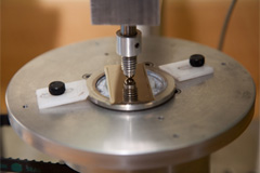
 This technique can be used to study the mecanical properties of coatings such as hardness, adhesion or resistance to delamination. During the tests, an indentation (Vickers) or a scratch is made on the surface of the sample using a diamond or tungsten carbide stylus. Tribological measurements can also be performed by moving back and forth and measuring the charge needed to start deteriorating the sample (critical charge).
Uses
- Measure the scratch resistance and adhesion
- Mesure microhardness
Application examples
- Research and development of coatings
- Measure the hardness of metallic samples
Technical specifications
Force: 3 mN to 30 N
Depth resolution: 0.1 µm
Lateral resolution: 10 µm
Manufacturer: CSEM
Model: MST Microscratch Tester
 Nano-indentation is the ideal technique to study the mechanical properties of very thin films (less than 1 µm) without the influence of the substrate. In this method, a small load is applied to a narrow indenter that penetrates the surface of the material. During the experiment, one monitors the depth penetration as a function of the load. The information collected then serves to determine the nanohardness, Young’s modulus, wear resistance or toughness of the material.
Uses
- Determine the nano-hardness
- Measure wear or scratch resistance
- Measure Young’s modulus
- Measure toughness
Technical specifications
Force : 10 µN – 10 mN
Depth resolution : 0.1 nm
Lateral resolution : 100 nm
Manufacturer : Hysitron
Model : TriboIndenter
 Tribometry is the study of frictional forces. The GCM has a “pin-on-disk” device to ascertain the wear rate in dry and liquid media. The sample is put on a disk rotating at a given angular speed. A ball fixed to a vertically-moving stem is pressed on the surface under study for a fixed number of disk rotations. The tangential force and vertical forces are measured, and the wear rate and the frictional coefficient can therefore be deducted.
Uses
- Measure the wear rate
- Measure the frictional coefficient
Technical specifications
Force : 0.03 – 50 N
Manufacturer : Functional Coating and Surface Engineering Laboratory (FCSEL)
Model : « pin on disk » type
Force : 0.03 – 50 N
 During this test, an adhesive band fixed to the coating is pulled at a constant rate (cm/min) by an increasing force until a failure occurs. The adhesion force is then obtained as a function of time. This apparatus is also useful to measure the frictional coefficient.
Uses
- Measure the adhesion force
- Determine the frictional coefficient
Technical specifications
Force : 0.1 – 50 N
Manufacturer : Instrumentors
Model : SP-103B
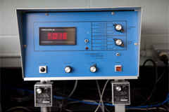
The GCM possesses a Tencor instrument to carry out intrinsic and thermal stress measurements for stresses between 0 and 20 GPa and temperatures between 20 and 900 °C. This apparatus measures the radius of curvature of circular substrates (prior to and after deposition) by laser interferometry. The stress values are then calculated from Stoney’s formula, knowing the thicknesses of the deposit and the substrate, as well as their respective Young’s moduli and Poisson coefficients.
Uses
- Measure thin film intrinsic stress
- Determine thermal stress in coatings
Technical specifications
Force : 0 – 20 GPa
Manufacturer : Tencor
Model : Flexus 2900
Throughout the years, the GCM has contributed to the success of companies in many different industrial sectors. To learn more about the innovative solutions that we propose to companies and a description of past projects.
 L’industrie aérospatiale se distingue par son utilisation des matériaux dans des conditions extrêmes. En effet, autant les conditions environnementales de température et d’humidité que les contraintes mécaniques imposent aux matériaux des stress énormes. Des traitements de surface tels que l’application de revêtements anti-corrosion ou anti-usure permettent d’améliorer de façon notable la longévité des matériaux utilisés en aérospatiale. En collaborant étroitement avec les leaders canadiens de l’aérospatiale, GCM Lab s’est doté d’une gamme de solutions uniques pour répondre aux besoins spécifiques de cette industrie. De l’analyse de défaillance à la caractérisation de contaminants, GCM Lab se démarque par ses services précis et professionnels.
Exemples d’application
- Concevoir et fabriquer des revêtements anti-érosion
- Déterminer la composition chimique de revêtements thermiques sur des pales de moteurs d’avions
- Mesurer la contamination dans des alliages de magnésium entrant dans la structure d’un avion
- Développer des microsystèmes pour le contrôle de l’intégrité d’aéronefs
- Caractériser les contaminants dans des pièces de carbone utilisés dans les systèmes de freinage d’avions
- Mesurer le délaminage de couches minces sur les avions
- Étudier les impuretés dans des composantes de satellite
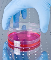 Dans le domaine médical, la qualité des produits se définit largement en termes de propreté, de biocompatibilité et de résistance à la corrosion. Des dispositifs médicaux tels que des cathéters, des verres de contact ou des endoprothèses doivent être complètement dépourvus de contaminants pour avoir un fonctionnement optimal. Une autre application biomédicale d’intérêt est l’étude de protéines et d’autres composés organiques pour la conception de biosenseurs et pour la croissance cellulaire. Dans ce contexte, GCM Lab est fier d’appuyer les industries pharmaceutiques et biomédicales en offrant une gamme complète de tests d’analyse chimique, de topographie de surface ou d’identification d’impuretés.
Exemples d’applications
- Analyser la contamination sur des appareils médicaux
- Cartographier la surface de polymères
- Analyser les couches d’un comprimé médicamenteux
- Profiler en profondeur des polymères
- Analyser des défaillances
- Déterminer la composition de couches minces
- Évaluer la qualité de l’acier inoxydable électropoli
 Le personnel de recherche ainsi que les techniciens de GCM Lab utilisent des appareils de haute technologie pour caractériser une large gamme de métaux, d’alliages ainsi que leurs revêtements. En plus de la caractérisation, nous détenons des capacités uniques en conception de revêtements fonctionnels pour limiter l’usure et la corrosion. Nos laboratoires renferment tout l’équipement analytique nécessaire pour mener à bien des études poussées de composition chimique, d’identification d’inclusions ou de topographie de surface.
Exemples d’application
- Identifier une source de corrosion
- Concevoir un revêtement anti-usure ou anti-corrosion
- Évaluation de la pureté de métaux
- Identification d’alliages inconnus
- Détermination de la concentration en plomb en surface pour des applications biomédicales
- Mesurer la concentration de nickel toxique à la surface de NiTi
La demande pour les sources d’énergies renouvelables croît à une vitesse exponentielle. Dans le cas de l’énergie solaire, d’énormes ressources sont dédiées à l’optimisation des matériaux photovoltaïques pour accroître le rendement global des panneaux solaires. C’est là où les techniques d’analyse de surface peuvent fournir de précieux renseignements sur la provenance d’impuretés ou la présence de défauts. Ces informations peuvent ensuite servir à améliorer le processus manufacturier et en réduire d’autant les coûts.
EXEMPLES D’APPLICATION
- Identifier des contaminations
- Mesurer l’indice de réfraction d’un revêtement optique par ellipsométrie
- Identifier des contaminants organiques sur semiconducteur
- Mesurer avec précision l’épaisseur de couches de c-Si, α-SiGe, α-SiGe, CdTe…
- Évaluer la quantité de dopant et son profil en profondeur
- Examiner l’orientation et la structure d’une couche mince
The microelectronics industry produces components with very high standards of cleanliness and reliability. A defective component or a contaminant can severely hinder the functioning of a printed circuit. Thanks to a large pool of equipment for chemical surface analysis, GCM Lab can easily identify any contaminant. Moreover, we offer to companies specialized in circuit assembly consulting services to improve the adhesion of electronic components on boards.
APPLICATION EXAMPLES
- Measure the surface conductivity
- Evaluate the surface topography
- Identify a contaminant
- Optimize the adhesion of electronic components
- Depth profiling of a semiconductor

New devices incorporating the latest optical technologies enter every day in our lives: DVD recorder, plasma screens, projectors, etc. The optics and photonics business is characterized by a high level of precision for the thickness of optical coatings, the purity of the materials used, etc. The GCM offers a large array of services especially suited for this industry: measurement of the index of refraction or the thickness of optical coatings, surface chemical analyses, roughness measurement of a lens, etc. Our expertise also includes the design of custom coatings for optical filters and anti-reflection applications.
APPLICATION EXAMPLES
- Measure the roughness of an optical coating
- Determine the index of refraction or the thickness of a coating
- Determine the chemical composition of an optical fiber
- Design optical filters
- Design anti-reflection coatings

The analytical capabilities of the GCM enable us to quantify many parameters in water or oils. For example, we can identify an oil or determine the composition of a contaminant in a liquid sample. Furthermore, our laboratories are equipped to measure the resistance of coatings or materials to erosion and corrosion. We also have instruments to measure many physical characteristics of coatings such as adhesion and roughness. Our leading edge facilities in microscopy also provide fundamental data for the identification of inclusions, surface topography, etc.
APPLICATION EXAMPLES
- Determine the composition of an oil
- Identify a contaminant
- Design a corrosion-resistant coating
- Measure grain size
- Determine coating thickness
- Examine surface topography
- Failure analysis

With an aging population to it must minister to, the pharmaceutical industry is expanding at a rapid pace. Pharmaceutical companies come up daily with new ways to produce effective drugs, with minimal side effects for the patient. In this context, the development and manufacturing of drugs must follow rigorous procedures. The surface analytical techniques to evaluate new biomolecules or identify contaminants then become necessary tools to ensure the quality of these developments.
The GCM offers a group of analytical and R&D services especially suited to the pharmaceutical industry. The diversity of our facilities and the competence of our personnel will help you to put in place reliable manufacturing processes, while minimizing the number of rejects. Our services include organic and inorganic techniques to identify impurities and to quantify a given element in each layer of a pill.
APPLICATION EXAMPLES
- Identify polymorphs
- Identify contaminants in products
- Analyze the chemical composition of each layer in a time-released drug
- Carry out a materials analysis on drug-delivery systems like inhalers

We combine our competence in polymers with several decades of experience to offer unique solutions to our industrial customers. Our expertise covers the chemical analysis of many types of polymers and plastics, surface analysis as well as failure analysis. Our laboratories include advanced instruments to deposit functional coatings on a wide range of polymers to improve their mechanical, thermal or chemical properties. All our personnel contributes to make each project a success, whether it be for a single measurement or a large-scale R&D project.
APPLICATION EXAMPLES
- Deposit coatings on polymers
- Analyse the surface of a polymer by microscopy
- Evaluate incoming materials
- Chemical analysis of a polymer
